Despite its numerous advantages, the use of InP in high-speed optical devices does come with challenges. The production process for InP can be complex and costly, which may limit its widespread adoption. Here are some key properties of Indium Phosphide (InP): Here are the key advantages of using Indium Phosphide: Superior Electron Velocity: InP boasts a much higher electron velocity compared to silicon (Si) and gallium arsenide (GaAs), approximately 5 times greater. Direct Band Gap: This property. Indium phosphide is a photonic integrated circuit (PIC) material suited for active functionalities. Beyond passive light routing, it can generate, amplify and detect light. Read on this page to learn more about indium phosphide characteristics, applications, and its comparison to other PIC. Indium Phosphide (InP), a duo-semiconductor born from the union of indium and phosphorus, has been thrust into prominence within the optoelectronics arena. Indium phosphide (InP) diodes are emerging as a promising semiconductor material for optoelectronics applications due to their. Abstract—A summary of photonic integrated circuit (PIC) platforms is provided with emphasis on indium phosphide (InP). Examples of InP PICs were fabricated and characterized for free space laser communications, Lidar, and microwave photonics. A novel high-performance hybrid integration technique.
[PDF]
This breakthrough technology dramatically reduces the number of external optical components, cutting the number of lasers required per module by half, simplifying optical module design and enhancing cost and supply chain efficiency for AI and data center applications. MIGDAL HAEMEK, Israel, March 10, 2025 – Tower Semiconductor (NASDAQ/TASE: TSEM), a leading foundry of high-value analog semiconductor solutions, and Innolight, a global leader in high-speed optical transceivers, today announced their expanded collaboration utilizing Tower's newest Silicon Photonics. Inno Semiconductor Technology, established in 2021, is located in Jiading District, Shanghai, China. Inno Semiconductor Technology is committed to promoting the commercialization of heterogeneous integrated material substrate. At present, our main products include high-performance micro acoustic. MIGDAL HAEMEK, Israel, Sept. 8, 2023 —Tower Semiconductor and data center optics company InnoLight Technology will develop multigeneration high-speed optical transceivers based on Tower's silicon photonics process platform. InnoLight Technology has been a leading infrastructure enabler of cloud data centers, wireless networks, fiber-to-the-home, and metro up. InnoLight 400G/800G optical transceivers aimed at AI interconnect. China's InnoLight Technology (Suzhou) Ltd. (Migdael Haemek, Israel). The partnership is.
[PDF]
One key aspect of this progression is the advent and evolution of transceivers, specifically SFP, SFP+, SFP28, QSFP+, and QSFP28. Let's delve into each of these technologies to understand their specifications, differences, and applications. A Cisco compatible SFP list 2026 represents a validated inventory of optical transceivers that utilize Multi-Source Agreement (MSA) standards to provide identical functionality to Cisco Original Brand (OB) optics. Deploying these modules allows network architects to reclaim up to 80% of their. —— Explosive Growth of 800G/1. 6T Technologies, Scene-Based Selection + Finisar Original Solutions in One Stop In 2026, driven by AI computing power, optical modules have entered a critical era of rate iteration, technological restructuring, and scenario segmentation. 800G has become the mainstream. Choosing the right Small Form-factor Pluggable (SFP) transceiver is critical for network engineers and procurement specialists aiming to optimize performance, cost, and reliability. This SFP buying guide offers a detailed technical comparison, real-world deployment insights, and practical selection. ity with compelling economics. Our ONE Network platform simplifies management of Cambium Networks' wired and wireless broadband and network edge technologies. Our customers can f iness rather than the network. We mak. SFP+ 10G ZR is designed for stable 80km single-mode transmission where standard 10G optics fail.
[PDF]
Silicon is to with wavelengths above about 1.1 micrometres. Silicon also has a very high, of about 3.5. The tight optical confinement provided by this high index allows for microscopic, which may have cross-sectional dimensions of only a few hundred. Single mode propagation can be achieved, thus (like ) eliminating the problem of.
[PDF]
Silicon photonics is transforming AI computing by enabling energy-efficient, high-speed data transmission. Discover how optical interconnects present a possible solution to the data center energy crisis and drive sustainable innovation. Lam Research is setting the agenda for the wafer fabrication equipment industry's approach to a silicon photonics revolution, driving the breakthroughs in Specialty Technologies that will enable sustainable AI scaling through precision optical manufacturing. The artificial intelligence boom has. y with vastly reduced energy con-sumption by integrating optics deeply within computing sockets. We present the design and characterization of a dense wavelength-division multiplexing (DWDM) SiPh transceiver chip, featuring a unique architecture in the multi-FSR regime and targeting a shoreline. Silicon photonics is becoming a critical enabler of AI and HPC, breaking the limits of electrical interconnects in bandwidth, distance and power efficiency. Co-packaged optics (CPO) builds on silicon photonics, with SiPh transceivers as the integration platform and CPO as the packaging architecture. Silicon Photonics emerges as the solution to this predicament, replacing electrons with photons—the fundamental particles of light—to race across familiar silicon-based chips, promising a revolution in computing and communication. This isn't just about increased speed; it's about a profound impact.
[PDF]
Explore our comprehensive SFP optical module selection guide for 2025. Learn about crucial factors like data rate, distance, fiber type, and compatibility to optimize your network performance and cost-effectiveness. Make informed decisions for your networking needs today!. SFP (Small Form-factor Pluggable) is a compact, hot-pluggable network interface module used to connect network devices (switches, routers, firewalls) to fiber optic or copper cables. They're essential for extending network distances and increasing bandwidth capabilities. Selecting the correct SFP module is not simply a matter of matching connectors. In modern Ethernet networks, choosing the wrong transceiver can result in link failures, speed mismatches, compatibility errors, or unexpected distance limitations. For network engineers, system integrators, and IT. At the core of these advanced networks are bidirectional SFP modules, also known as BiDi SFP transceivers—compact, cost-efficient devices that support high-speed data transmission and reception over a single optical fiber. By using different interfaces and single-mode or multimode fiber depending on the.
[PDF]
Laser diodes without feedback photodiodes are common in laser pointers, barcode scanners, CD/DVD/Blu-ray players, laser toys and simple alignment tools. The laser diode is an unsung hero of modern technology. Diode laser technology drives a. An example of an edge-emitting laser diode structure is shown in Figure 1. This type of structure is termed to as Fabry-Perot type laser. From the figure above, you can clearly see that a PN junction is formed by two layers of doped gallium arsenide (GaAs). Each type of laser diode is designed for specific applications, so choosing the right one ensures you achieve the best results for your needs. 3 Ready to find the perfect laser for your job?. A laser diode, manufactured by Electronic Spices, is a semiconductor device known for its ability to emit coherent light through a process called stimulated emission. Laser diodes are widely used in various applications such as fiber-optic communications, barcode readers, laser pointers. Laser diodes (LD) are semiconductor devices that convert electrical energy into high-power optical energy. These devices are currently used in the fields of telecommunications and medicine and in industrial cutting and welding applications. What is a Laser Diode? The term LASER stands for Light Amplification by Stimulated Emission of Radiation.
[PDF]

Optical amplifiers work differently. They amplify the light directly, with no conversions. This process is faster, more efficient, and keeps the signal clearer. Using optical amplifiers helps reduce signal distortion, lowers system costs, and supports long-distance communication. The most common types include: Erbium Doped Fiber Amplifiers (EDFA): EDFAs are the most commonly used type of optical amplifier in telecommunications. They play a vital role in modern optical communication systems, enabling the transmission of high-speed data over long-haul networks. An optical amplifier is a device that boosts the strength of an optical signal. 2dB per kilometer for 1. This means that over a distance of 100km, a signal can lose around 20dB. This principle dictates that a photon can interact with an atom already in an excited energy state, forcing the excited atom to immediately release its stored energy as a second photon. It does this without changing the light into an electrical signal. In the past, systems used repeaters to fix weak signals. These repeaters turned light into electricity, boosted the signal, and then. The SPIE Digital Library offers a comprehensive range of content on optical amplifiers, reflecting their significance in modern photonics and telecommunications. The library includes a variety of peer-reviewed papers, conference proceedings, and technical articles that delve into the fundamental.
[PDF]
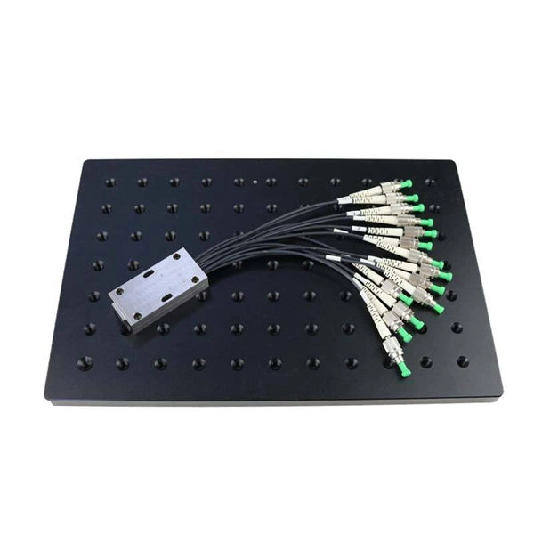
While traditional fiber optic cables contain individual fibers encased in a protective jacket, ribbon fiber cables organize fiber optic strands in a flat ribbon structure, creating freedom with space conservation and cable management. Data Centers: The flexible ribbon cables deliver phenomenal bandwidth between densely packed servers and networking gear in data centers. Motor Meter: Ribbon cables can be used to connect the control circuitry to the display or to the motor drivers. Telecom Devices: In telecommunications, flat. Ribbon cables offer higher fiber counts and greater fiber density than any other cable construction designed for the outside plant (OSP), four times the highest-fiber-count loose tube cable. Ribbon cables also enable mass-fusion splicing, whereby each 12-fiber ribbon can be spliced in a single. The technology of ribbon fiber optic cables is well-established in the telecommunications industry and is favored for its high fiber density and compact size. Join us as we embark on a journey of discovery, demystifying the technology that has changed the way we connect and communicate. Welcome to the world of Ribbon Fiber Optic Cables. One of our most innovative technologies is the ribbon fiber optic cable —a compact, powerful solution that is transforming the way organizations manage high-density connections while optimizing valuable space. In this article, we'll delve into why ribbon fiber optic cables are a game-changer, how.
[PDF]
An optical transport network (OTN) is a digital wrapper that encapsulates frames of data, to allow multiple data sources to be sent on the same channel. This creates an optical virtual private network for each client signal. ITU-T defines an optical transport network as a set of optical network elements (ONE) connected by optical fiber links, able to provide functionality of transport, multiplexing, swit. EquipmentAt a very high level, the typical signals processed by OTN equipment at the Optical Channel layer are: • SONET/SDH• Ethernet/FibreChannel• Packets. • - Details of all OTN areas including breakdown of the full frame Anritsu Poster - Details of all OTN areas including breakdown of the full frame at the Wayback Machine (archived 2014-05-17)•.
[PDF]